An array of individually addressable microscale optical resonators that offer higher resolution, lower power consumption, extremely rich color tones, and a unique manufacturing path.
Problem:
Current display devices, with either active or reflective displays, are limited by high power consumption, inadequate resolution, and limited viewing angles. Moreover, these technologies allow control over the amplitude or phase of light, but not both.
Solution:
The current invention offers a reflective display that reduces power consumption and increases resolution while making the device easier to operate outdoors. Since each optical resonator is individually addressable, both phase and amplitude can be controlled.
Technology:
The invention consists of a series of optical cavities, each with a bottom layer of silicon mirror and a top film of Platinum (Pt) that is partially reflective. The two layers are separated by a thin gap typically filled with water. The top layer can be tuned using a voltage that causes the layer to expand and subsequently alter its spectral reflectance. Incident light is reflected by the bottom mirror and partially by the top layer, which is further split by the bottom mirror, forming an optical resonator. The thickness of the top layer, as controlled by the voltage, determines the wavelength of light reflected by the optical resonator.
Advantages:
- The device requires a power source of less than 1V (estimated 0.2V), so it would use less power and extend battery life over current display technologies
- Increased resolution with pixel size 1-10 microns, well below the resolution limit of human vision, compared to 10-100 microns pixel size of current display technology
- Each pixel can operate within voltage range (~1V) and switch at speed upwards of 100msec
- The device is manufactured using atomic layer deposition, which decreases the size of each pixel. Nearly 10,000 pixels fit within the smallest space resolvable to the naked eye, almost 10-fold smaller than current technologies.
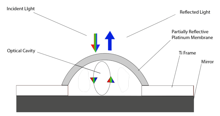
A schematic cross-section of the device. The device consists of a bottom layer that is a mirror and a top Pt layer that is semi-reflective. Incident light is reflected by the bottom and top layers, forming an optical resonator. The user can tune the voltage in the resonator to modulate the color of light reflected.
Desired Partnerships:
- License
- Co-development: with cell phone manufactures or specialized optics manufacturers (Thorlabs, Edmund, Nikon, etc.)
Case ID:
22-10112-tpNCS
Web Published:
5/12/2023
Patent Information:
| App Type |
Country |
Serial No. |
Patent No. |
File Date |
Issued Date |
Expire Date |