A design and method to create superlattices, alternating stacks of two-dimensional materials and semiconductors to obtain strong light absorption.
Problem:
Next-generation optical technologies like light detection and ranging (LiDAR) and on-chip optical modulators have wide-ranging applications in autonomous vehicles, device communication, and computing. Unfortunately, existing technologies are hampered by their sensitivity, often requiring specific substrates and operating environments. Two-dimensional materials like transition metal dichalcogenides (TMDs) have highly desirable optical and electronic properties for such applications, but offer uneven sample thickness, small lateral dimensions, and weak light absorption.
Solution:
The researchers developed a method to create semiconductor-TMD superlattices. These superlattices offer controllable thickness, device-scale lateral size, and strong light absorption. In addition, they maintain the quantum effects found in TMD monolayers such as exciton-polariton splitting. This introduces exciting avenues for optical device engineering.
Technology:
TMDs offer an excellent platform for optical devices due to their direct bandgap, strong quantum confinement, and nonradiative exciton-hole energy loss. The authors were inspired by these benefits to devise a method to harness TMDs’ upsides while mitigating the downsides of sample preparation and geometry. They accomplished this by stacking TMDs and thin semiconductors together using a wet chemical transfer process. This stabilizes the TMDs and enables quantum device designs on the order of square centimeters.
Advantages:
- Method creates samples on the order of 1 cm2 for real-world device applications
- Superlattices exhibit over 80% light absorption at TMD excitonic frequency
- Preserves quantum effects of the monolayer TMDs, including exciton-polariton Rabi splitting up to 170 meV
- Cavity mode quality factor as large as 300
- Operates at room temperature
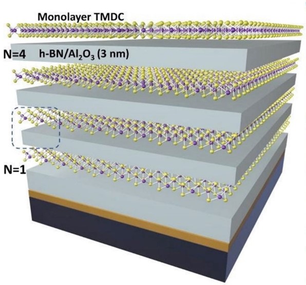
Structure of a superlattice combining 2D TMD sheets with nanometer-scale semiconductor slabs. Such a superlattice offers over 80% light absorption at the TMD exciton peak and hosts interesting quantum effects like exciton-polariton splitting.
Case ID:
21-9665-tpNCS
Web Published:
5/12/2023
Patent Information:
| App Type |
Country |
Serial No. |
Patent No. |
File Date |
Issued Date |
Expire Date |