A flexible photonics processor enabling on-chip optimization of light-speed information processing without requiring complex fabrication.
Problem:
Integrated photonics processors allow for high-speed transmission of large-bandwidth data with unlimited parallelism. However, these integrated photonics processors require intricate construction, necessitating costly and sensitive lithography. Further, these devices require exponentially complex architectures as they are scaled up for modern, large dataset technologies. In addition, existing platforms are static and require error-prone lithographic manufacturing, limiting yield. To meet the information processing requirements necessary to advance large scale technologies like artificial intelligence, improved computing power by eliminating the information transfer and manufacturing constraints of traditional processors is required.
Solution:
A lithography-free method to generate an integrated photonics processor that allows for reconfigurable control of an imaginary index on a semiconductor platform. This allows light-speed information transfer without the energy loss or heat generation of electrical processors. Using spatially distributed optical gain and loss, the device mimics complex lithographic pathways, creating flexible optical “circuits” without the need for expensive and highly precise manufacturing. Because of this flexibility, these pathways can be optimized via on-chip training to shape the processor to the specific application. This reconfigurable integrated photonic processor outperforms current methods by providing the potential to process large, non-local datasets with the throughput necessary for modern artificial intelligence applications.
Technology:
Dynamically altering spatial patterning of optical gain across a central unpatterned slab of III-V semiconductor provides the basis for circuit construction. Optical coding of patterned light delivered by a spatial light modulator (SLM) defines the gain and loss distribution across the semiconductor wafer, spatially modulating an imaginary index that takes the place of a real index constructed by lithography. This approach allows for optical coding and real-time feedback, enabling on-chip training and flexible configuration by algorithmic optimization of matrix elements.
Advantages:
- No requirement of highly precise lithography for construction
- Flexible information processing architecture
- Compact, 21x smaller footprint than conventional platforms
- 14 THz bandwidth
- Lossless transmission of optical signal
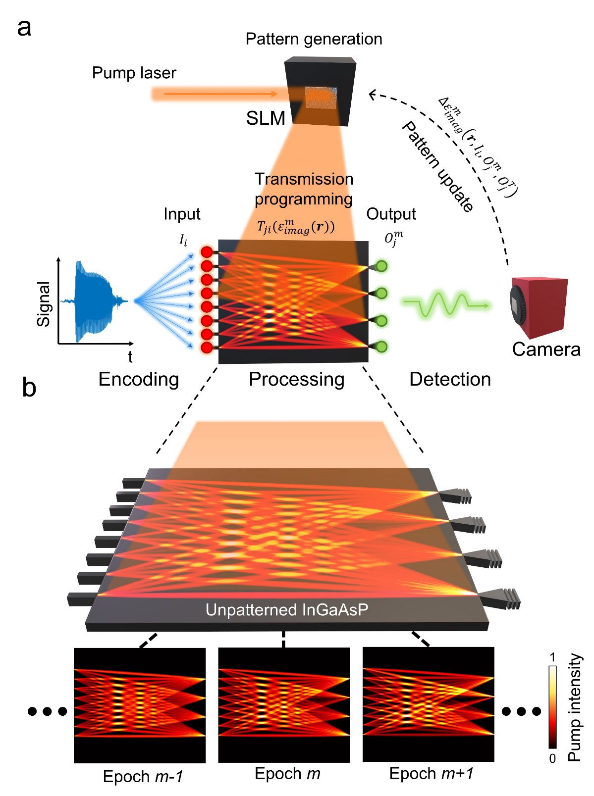
Depiction of the lithography-free photonics processor. (a) An imaginary index created via a pattern generated by a spatial light modulator (SLM) onto a wafer of unpatterned indium gallium arsenide phosphide (InGaAsP). (b) This allows the processing scheme to be reconfigurable without the need for complex lithographic manufacturing.
Case ID:
23-10393-tpNCS
Web Published:
2/5/2024
Patent Information:
| App Type |
Country |
Serial No. |
Patent No. |
File Date |
Issued Date |
Expire Date |