A Quadrature Delay-Locked Oscillator that caters to increasing multi-GHz and multi-phase clock demands in systems such as time-interleaved architectures.
Problem:
The unrelenting growth of artificial intelligence (AI) requires advancements in high-performance hardware capable of delivering high-speed clock generation and distribution. These improvements are essential to accommodate the increasing demand for growing data rates. Traditional complementary metal-oxide semiconductor (CMOS) electronics experience significant dynamic power dissipation and losses at high frequencies (multi-GHz) due to frequent charging and discharging of capacitive loads combined with parasitic resistances. Additionally, variations in wire resistance, capacitance, and power supply fluctuations introduce timing uncertainties, affecting synchronization (clock skew and jitter). As clock frequencies increase, undesirable effects such as crosstalk and electromagnetic interference (EMI) become more pronounced, leading to degraded signal quality, poor confinement, and high loss.
Solution:
The inventors developed an electronic-photonic quadrature delay-locked oscillator (DLO) capable of producing 4-phase optical clock signals suitable for on-chip optical clock distribution. This platform technology can produce a clean, multi-phase frequency reference in the optical domain. Rather than use an external crystal oscillator to stabilize an oscillator (as traditional in a phase-locked loop), the proof-of-concept DLO utilizes fixed optical delay references. The entire system is capable of being monolithically integrated on today’s modern CMOS silicon-photonics platforms (such as
GlobalFoundries 45SPCLO Fotonix process). The ability to integrate a high-quality reference on-chip allows for the reference to track the variations of other on-chip components, enabling exceptional device matching and timing alignment at lower system size, weight, and power. Compared to traditional electronic circuitry, this solution could lead to enhanced signal fidelity and synchronization over a wide range of frequencies.
Technology:
The distinguishing innovation of the DLO is the use of (a) fixed (optical) delay reference(s) to stabilize a variable frequency oscillator, such as a voltage-controlled oscillator (VCO). Traditionally, a phase-locked loop (PLL) or delay-locked loop (DLL) is used for frequency synthesis and clocking applications. A PLL uses a variable frequency block to lock its output to a fixed frequency reference. A DLL uses a variable delay block to lock its output to a fixed frequency reference. The novel DLO uses a variable frequency block to lock its output to a fixed delay reference, distinguishing itself from the ubiquitous PLL and DLL. Delay is implemented optically rather than electrically, as low-loss delay is easy to produce in the optical domain and is relatively immune to process, voltage, and temperature (PVT) variations. The optical outputs facilitate clock routing through large, wafer-scale chips using on-chip photonic waveguides. The product offers potential customization to create arbitrary n-phase outputs, the ability to adapt for tunable delay references, the ability to interface seamlessly with other photonic systems, and the ability to use a reference which tracks other on-chip components and qualities.
Advantages:
- The DLO offers the ability to create a frequency reference which tracks the temporal period, τ, of an optical delay line.
- Optical signals are more immune to PVT variations compared to electronic counterparts.
- DLO architecture is capable of being entirely monolithically integrated in a CMOS silicon-photonics process, reducing cost, size, weight, and power.
- Optical clock edges do not degrade over long distances and thus obviate the need for many localized clock recovery blocks.
- High frequency optical routing is much easier than electrical routing.
- Optical routing is extremely wideband, low-loss, and not prone to EMI or crosstalk.
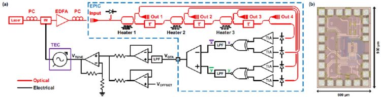
The system architecture is shown in Figure (a). A C-band (1550nm) laser source is first modulated by a VCO using an electro-optic intensity modulator. The modulated optical signal is coupled to an input grating coupler which feeds into a four-tap optical delay line. The four-tap optical delay line is used to create four identical optical signals that are evenly spaced in time by τ. On-chip tunable directional couplers are used to equalize the optical outputs. While half the optical output is sent to output grating couplers for monitoring, the other half is sent to on-chip photodiodes (PD) and resistors for I-to-V conversion. Limiting amplifiers are used to condition the signals before phase detection is performed by digital CMOS XNOR gates followed by low pass filters (LPF). An operational transconductance amplifier (OTA) in the negative feedback configuration enforces the loop to lock at the point where the average values of both phase detector outputs are equal, corresponding to a frequency of 1/(4τ) Hz. An additional LPF is used at the output of the OTA to improve stability and to filter the noise. In this implementation, the target off-chip VCO supports an input tuning voltage between 0 V and 12 V. Since the output of the on-chip OTA is limited between 0 V to 1.8 V, a summing amplifier is used to level-shift the OTA output and provide additional loop gain. In this case, the offset voltage can be set such that the loop locks and, as a result, the frequency drift of the VCO over temperature is reduced. Figure (b) is the micrograph of the Electronic Photonic Integrated Circuit (EPIC) with dimensions of 600µm X 900µm.