Synthesis of epitaxial two-dimensional Indium(II) selenide (InSe) by metal-organic chemical vapor deposition (MOCVD) over 2-inch wafers and its applications in electronics.
Problem:
The current methods have not demonstrated the large-area synthesis of 2D InSe due to the complexity of the binary In-Se system and the difficulties in promoting lateral growth. In conventional chemical vapor deposition (CVD), it has been difficult to balance the flux ratio between In and Se needed to achieve layer-by-layer growth.
Solution:
The solution is to create epitaxial 2D InSe by metal-organic chemical vapor deposition (MOCVD) over 2-inch wafers. This epitaxial growth of InSe on c-plane sapphire is performed via precursor flow modulation to control the Se/In flux ratio. This growth happens layer-by-layer for thickness control over wafer scales with tunable optical properties compared to the bulk crystals.
Technology:
The polymorph-selective, high-quality, and thickness-controlled 2D InSe thin film is grown through vertical, cold-walled MOCVD shown in Fig 1. The Se source is periodically interrupted during flow-modulated MOCVD, so that an Se-deficient environment is created that favors the nucleation of InSe over In2Se3. The resulting crystalline InSe domains are directionally oriented along the crystal structure of the substrate, and the thickness of InSe can be controlled as a function of growth time.
Advantages:
- The layer-by-layer growth allows thickness control over wafer scales
- It has tunable optical properties comparable to those of bulk crystals
- Gate-tunable electrical transport with a field-effect mobility comparable to single-crystalline flakes is also demonstrated.
- Provides better precursor control and mass production for large-area applications
- Creates few-layer InSe transistors with a high on-to-off current ratios (Ion/Ioff ratio ≈10^4-10^5) and two-terminal field effect mobility (μFE ≈2.8 cm2V-1s-1).
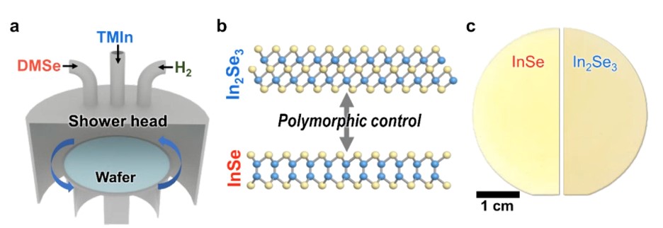
Figure-1: a) Schematic of MOCVD system, Dimethyl selenide [DMSe; (CH3)2Se] and trimethylindium [TMIn; (CH3)3In] are used as the Se and In precursors. b) Schematic crystal structures of indium selenide polymorphs c) ) Photographs of the monolayer InSe (left) and In2Se3 (right).
Case ID:
23-10361-TpNCS
Web Published:
6/12/2026
Patent Information:
| App Type |
Country |
Serial No. |
Patent No. |
File Date |
Issued Date |
Expire Date |